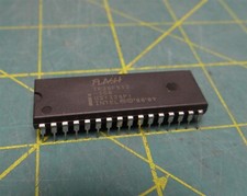
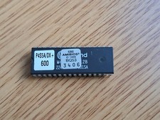
We can program this chip for you for FREE if you can provide us with the needed BIOS firmware for your vintage PC motherboard.
NOTE: NOT ALL CMOS CHIPS ARE THE SAME INTERNALLY. THEY MAY HAVE THE SAME SPECIFICATIONS (ie 2M-bit 256k x 8-bit) BUT CAN HAVE DIFFERENT PIN LAYOUTS OR STORE DATA IN DIFFERENT AREAS OF THE CHIP CAUSING THEM NOT TO WORK CORRECTLY (no boot, beep codes, or failed 2nd re-boot) FOR YOUR MOTHERBOARD. ALWAYS TRY TO REPLACE YOUR CMOS CHIP WITH THE EXACT SAME MANUFACTURE AND PART NUMBER AS THE ORGINAL CHIP OTHERWISE YOUR TAKING A REAL GAMBLE.I cannot be held responsible should you choose the wrong chip for your application.
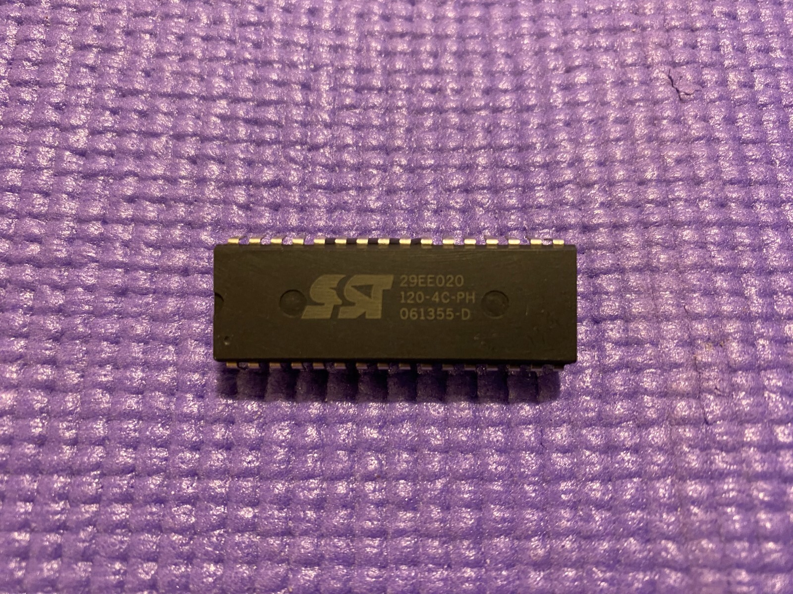
Your item will be professionally packaged using a foam lined hard clam shell to ensure no bent pins plus an outer anti-static bag. All chips are shipped in a brand new virgin craft 200lb rated cardboard box using pink anti-static foam peanuts.CMOS 32 pin DIP BIOS chip SST 29EE020 120-4C-PH 2M-BIT [256K x 8] CMOS FLASH MEMORY.(We can program this chip for you for FREE if you can provide us with the needed BIOS firmware for your vintage motherboard.)QUICK GENERAL DESCRIPTION:
PRODUCT DESCRIPTION
The SST29EE/LE/VE020 are 256K x8 CMOS Page-Write EEPROM manufactured with SST’s proprietary, high performance CMOS SuperFlash technology. The split-gate cell design and thick oxide tunneling injector attain better reliability and manufacturability compared with alternate approaches. The SST29EE/LE/VE020 write with a single power supply. Internal Erase/Program is transparent to the user. The SST29EE/LE/VE020 conform to JEDEC standard pinouts for byte-wide memories.FEATURES:
• Single Voltage Read and Write Operations
– 5.0V-only for SST29EE020
– 3.0-3.6V for SST29LE020
– 2.7-3.6V for SST29VE020
• Superior Reliability
– Endurance: 100,000 Cycles (typical)
– Greater than 100 years Data Retention
• Low Power Consumption
– Active Current: 20 mA (typical) for 5V and
10 mA (typical) for 3.0/2.7V
– Standby Current: 10 µA (typical)
• Fast Page-Write Operation
– 128 Bytes per Page, 2048 Pages
– Page-Write Cycle: 5 ms (typical)
– Complete Memory Rewrite: 10 sec (typical)
– Effective Byte-Write Cycle Time: 39 µs (typical)
• Fast Read Access Time
– 5.0V-only operation: 120 and 150 ns
– 3.0-3.6V operation: 200 and 250 ns
– 2.7-3.6V operation: 200 and 250 ns
• Latched Address and Data
• Automatic Write Timing
– Internal VPP Generation
• End of Write Detection
– Toggle Bit
– Data# Polling
• Hardware and Software Data Protection
• Product Identification can be accessed via
Software Operation
• TTL I/O Compatibility
• JEDEC Standard
– Flash EEPROM Pinouts and command sets
• Packages Available
– 32-lead PLCC
– 32-lead TSOP (8mm x 14mm, 8mm x 20mm)
– 32-pin PDIP



![[10 Pcs] Intel E28F010-120 CMOS FLASH MEMORY 32 PIN TSOP picture](/store/item/img/g/SG0AAOSwRU9nKa7A/s-l225/-10-Pcs-Intel-E28F010-120-CMOS-FLASH-MEMORY-32-PIN.jpg)